By Eric Stann
July 29, 2025
Contact: Eric Stann, StannE@missouri.edu
Photo by Abbie Lankitus
University of Missouri researchers have devised a more efficient and precise method for manufacturing computer chips.
Traditionally, engineers use a technique known as atomic layer deposition (ALD) to apply ultra-thin layers of material across a chip’s surface. But the process coats everything, even areas that should stay clean. Think of it like painting an entire house in one step — walls, ceilings and floors — but accidentally covering the windows, too.
That’s a problem when you’re working with chips packed with billions of microscopic switches, called transistors, that control the flow of electricity inside smartphones, laptops and other electric devices.
To address this challenge, the Mizzou team developed ultraviolet-enabled atomic layer deposition (UV-ALD). This method uses UV light to precisely control where a thin layer of material — often a metal oxide — is applied during fabrication. The metal oxide coatings help direct the flow of electricity through each transistor, improving the overall efficiency of the chip.
This targeted approach could reduce manufacturing steps, saving both time and materials.
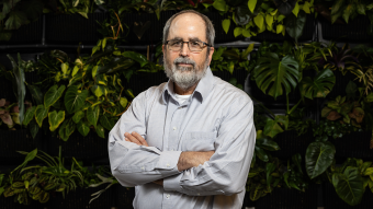
“Our process cuts the traditional four or five manufacturing steps down to just two,” said Matthias Young, an assistant professor with joint appointments in Mizzou’s College of Engineering and College of Arts and Science. “We make the surface ‘sticky’ using UV light and then apply the coating. It only attaches where the light has been applied.”
The new method could also benefit the environment.
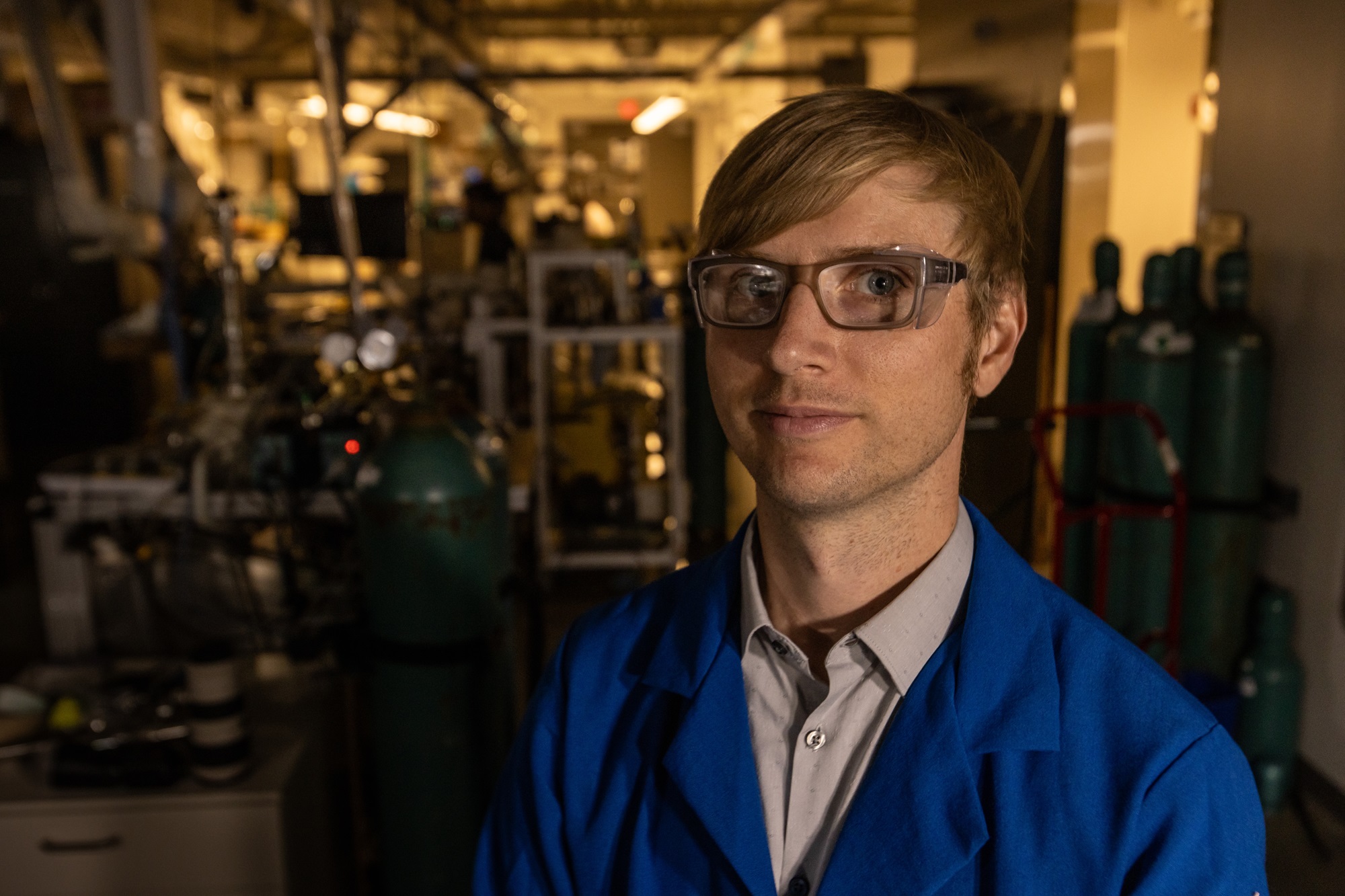
“With fewer steps, we reduce the use of harmful chemicals,” Andreas Werbrouck, a postdoctoral researcher and co-author of the study, said. “That’s safer for workers and better for the planet.”
In their work, the team demonstrated their approach on a new material, molybdenum disulfide (MoS₂), which may help build the next generation of chips.
The study, “Ultraviolet light-induced functional group formation on molybdenum disulfide for patterned atomic layer deposition,” was published in the journal Chemistry of Materials. Azeez Musa, Gordon Koerner, Nikhila Paranamana and Matt Maschmann at Mizzou also contributed to the work.
This work was done at the MU Materials Science and Engineering Institute (MUMSEI) — a partnership between the College of Engineering and the College of Arts and Science.